Comparison Between Light Microscope & Electron Microscope

Light microscope is an optical instrument that uses optical principles to magnify and image tiny objects that cannot be distinguished by the human eye, so that people can extract microstructure information. The application of electron microscopy technology is based on the basis of optical microscopy. The resolution of the light microscope is 0.2 μm, and the resolution of the transmission electron microscope is 0.2 nm, which means that the transmission electron microscope is magnified 1000 times on the basis of the light microscope.

Mechanism of image formation. Source: biologyexams4u.com

Electron microscopes can be divided into transmission electron microscopes, scanning electron microscopes, reflection electron microscopes and emission electron microscopes according to their structure and use. Light microscopes can be divided into trinocular microscopes and binocular microscopes according to the number of eyepieces; according to the stereoscopic image, they can be divided into stereoscopic and non-stereoscopic microscopes; according to the observation objects, they can be divided into biological and metallographic microscopes; according to optical principles It can be divided into polarized light, phase contrast and differential interference contrast microscopy.

The light microscope uses visible light as the medium, and the electron microscope uses the electron beam as the medium. Since the wavelength of the electron beam is much smaller than that of the visible light, the resolution of the electron microscope is much higher than that of the light microscope. The maximum magnification of an light microscope is only about 1500 times, and a scanning microscope can magnify more than 10,000 times.

According to the de Broglie wave theory, the wavelength of an electron is only related to the accelerating voltage:

λe=h / mv= h / (2qmV)1/2=12.2 / (V)1/2 (Å)

Under the accelerating voltage of 10 KV, the wavelength of electrons is only 0.12Å, which is much lower than 4000-7000Å of visible light, so the resolution of electron microscopes is naturally much better than that of light microscopes. However, the electron beam diameter of scanning electron microscope is mostly between 50-100Å, and the reaction volume of elastic scattering (Elastic Scattering) and inelastic scattering (Inelastic Scattering) of electrons and nuclei will be larger than the original electron beam diameter. Therefore, the resolution of the general transmission electron microscope is higher than that of the scanning electron microscope.

An important feature of scanning electron microscopes is that they have a large depth of field, which is about 300 times that of light microscopes, which makes scanning microscopes more suitable for observing samples with larger surface fluctuations than light microscopes.

For more information, please visit https://www.sputtertargets.net/.

Challenge in the Next Ten Years – Quantum Computing

For many people, these three things will bring us incredible challenges in the coming years: quantum computing, generalized artificial intelligence, and large-scale space travel will all be there. For now, quantum computing is on the verge of changing the world we live in forever, while the other two things are still in their infancy. In comparison, the biggest challenge in the next ten years, which is closer to us, is quantum computing.

Google and IBM, as well as other major players in the technology field, have proven the immediacy of quantum computing. They have invested a lot of money in quantum computing and are committed to creating a quantum computer that can surpass conventional computers. If this goal is achieved, dozens of long-standing problems are suspected to be suddenly solved by quantum computing-from curing Alzheimer’s disease and other previously incurable diseases to more accurately predicting financial markets.

However, unfortunately, as we approach a new era of solving technical problems, we will also face new network security issues because our current protective measures are outdated. Although this concern will not outweigh the huge benefits of quantum computing, every step needs to be carefully considered.

On this basis,I want to search for a scalable method of entanglement of the qubits. This element of the process allows a quantum computer to take into account all of the variables and their relationships when addressing a problem, making feats like predicting effects of climate change and creating life-saving medications possible.

Thus far, the focus has been on methods of facilitating entanglement that require extreme conditions, such as near absolute zero temperature ranges, to make quantum computing a reality.This has been necessary up to this point as our understanding of this groundbreaking technology grows. However, this is not feasible as a large-scale solution because of the cost and resources associated with maintaining those incredibly low temperatures. If quantum computing is to accomplish all of the life-changing feats it has the potential to, it will need to be accessible enough to be used by all the industries in question, both to use to solve those problems and to defend against cyber attacks in the process.

I would approach my research with the goal of offsetting the need for extreme conditions by either size or mechanical complexity. I would investigate different possibilities for preserving the immense power of quantum computing as the processes are scaled. This is a vital facet of the research to ensure quantum computing does not remain yet another form of technology available only to the wealthiest industries and therefore not used to its fullest potential.

Information from Stanford Advanced Materials.

Burning Plasma Nuclear Fusion: The Biggest Challenge and the Solution

As the demand for energy continues to increase, more and more greenhouse gases are released into the atmosphere. Clean energy is more important than ever to ensure our human survival on the planet. To this end, the European Union has set 2050 as the deadline for the complete decarbonization of global energy[1]. However, the road to achieve this goal is full of obstacles: solar energy requires a lot of space, wind and hydropower have relatively low output and can only generate energy in specific locations, and nuclear fission causes countless harms from nuclear waste to reactor accidents. When considering all the available options, the cleanest and safest way to power the world stood out: nuclear fusion.

Nuclear fusion involves placing a gas under immense heat and pressure, turning it into a plasma and fusing small atoms into larger ones, converting a small amount of mass into a large amount of energy. The energy produced by nuclear fusion is almost 4 million times that of burning coal, oil or natural gas, and about four times that of nuclear fission of the same quality. [2] Nuclear fusion does not release any greenhouse gases, but instead releases unstable nuclei that will remain radioactive for millions of years. It only produces inert helium. Fusion will not cause a nuclear accident, because unlike fission, it is not based on a chain reaction; if there is a problem with the reactor configuration, the plasma in the reactor will cool down and the reactor will automatically shut down within a few seconds. Fusion reactors cannot be used to make weapons because “although hydrogen bombs do use fusion reactions, they require additional fission bombs to detonate.” [3] Finally, fusion is achieved by the collision of deuterium and tritium, two isotopes of hydrogen. Deuterium can be produced from water and tritium from lithium, which is present in the ocean in trillions of metric tons, so “supply would not be a problem for millions of years.”[4]

Despite its incredible promise, nuclear fusion poses numerous technological issues, from confinement to plasma stability. [5] The “fundamental challenge” of fusion is to “make the fusion plasma emit heat faster than the energy velocity injected into the plasma”, and this is not yet accomplish. [6] The plasma must be kept at a high enough temperature so that the particles move so fast that they can get close enough to make the attractive force between the two nuclei effective and overwhelm the electrostatic repulsion. The solution to this problem is to create a self-sustaining “burning plasma”, which is “mainly heated by the energy generated by the fusion reaction occurring in the plasma, rather than heated by an external source.” [7] The fusion of deuterium and tritium produces a positive charge. Helium nuclei or alpha particles, and to achieve combustion plasma “At least 66% of the total heat [must] come from fusion alpha particles.” [8] This is the first step to unleash the myriad benefits of nuclear fusion, so I will study my research Focus on developing the first burning plasma ever.

The International Thermonuclear Experimental Reactor (ITER) is already making this effort. Existing research on combustion plasma has identified a number of technical challenges involved in its generation process. First, although the alpha particles released by fusion keep the plasma high, when present in large quantities, they can reduce the frequency of deuterium-tritium collisions, thereby cooling the plasma. Therefore, one of the main challenges in generating combustion plasma is to create an effective divertor to quickly remove helium from the reactor. [7] My research will focus on developing divertor materials that can withstand the heat of reaction and determining the correct removal rate to take advantage of the heating advantages of alpha particles without significantly reducing the frequency of deuterium-tritium collisions.

Another challenge is the development of a lithium-containing “blanket” surrounding the fusion core. In addition to alpha particles, fusion releases electrically-neutral neutrons, which produce heat and tritium when they collide with lithium. Both products can be used to sustain the reaction, maintaining high temperatures and replacing tritium consumed in fusion. The main challenges of blanket design include extracting tritium from the blanket, recycling it, and re-injecting it into the plasma.[7]

The third issue related to burning plasma involves density. That is, “increasing the plasma density is advantageous in principle because it increases the possibility of fusion reactions. However, as the density approaches its maximum value, many experiments have shown that the plasma confinement degrades more than expected.” One technique to solve this problem is machine learning: using statistical data and big data, artificial intelligence may be able to “identify important patterns and reveal information hidden in years of experimental data.”[8]

Mankind should treat issues such as climate change and nuclear war as issues to be resolved, rather than waiting for revelation. [9] And nuclear fusion power may be the solution we have been looking for. In the foreseeable future, nuclear power is not only the biggest solution; it is also the biggest challenge. But through the study of burning plasma, we can overcome this huge challenge and create a clean and self-sustaining response that will power the world for thousands of years.

Information from Stanford Advanced Materials.

References

  1. Jha, A. (2015, January 25). When you wish upon a star: Nuclear fusion and the
  2. Advantages of fusion. ITER. (n.d.).
  3. IAEA. (2016, October 12). Fusion – frequently asked questions. IAEA.
  4. Provide energy from fusion. Grand Challenges – Provide Energy from Fusion. (n.d.).
  5. Chatzis, I., & Barbarino, M. (2021, May 7). What is fusion, and Why is it so difficult to achieve? IAEA.
  6. Nuclear Fusion Power. Nuclear Fusion : WNA – World Nuclear Association. (2021, June).
  7. Baldwin, J. W. (n.d.). Fusion energy via magnetic confinement. Princeton University.
  8. Barbarino, M. (2021, May 6). Burning plasma. IAEA.
  9. Garfield, L. (2018, May 8). The author of Bill Gates’ favorite book suggests 9 big reasons the world is getting better. Business Insider.

Evaporation Pellets Used in Thermal Evaporation

Evaporation, or more specifically, Resistance Thermal Evaporation, involves the heating of the evaporation material within a vacuum environment. The materials used in vacuum evaporation are usually made into pellets, so they are also called evaporation pellets. These pellets are heated to a temperature above which the vapor pressure of the material exceeds that of the vacuum environment in which it is contained (more on this later).

The vacuum evaporation form is simple and the equipment required to produce the film is actually very small. First, like other PVD technologies, some type of vacuum system is needed to provide the right operating environment. Electrical energy must be supplied in the vacuum chamber, usually from a remote power source through a standard electrical feeder to the vacuum chamber, and then to the busbar via a busbar. A resistance source (evaporation source) is connected between the bus bar and the bus bar. The composition of the source may vary based on the particular material being evaporated. Typically, they are high-resistance wires or sheet materials shaped like “boat-shaped” (usually refractory metals) that are connected between the two electrodes to generate heat when powering the bus. By applying a current to the electrodes, the source material heats up and the vapor pressure increases. Once the vapor pressure of the material exceeds the vapor pressure of the background environment, vaporized molecules condense between the source material and the substrate and condense there to form a film.

Each material has a specific vapor pressure under any conditions. Generally, the higher the temperature (the power of the resistor source), the higher the deposition rate of the evaporated material. The vapor pressure of various materials is readily available in the literature and can be easily viewed via the Internet.

Unlike sputter coatings that eject a single atom or cluster at a time, thermal evaporation into a vapor stream can be quite robust, thus achieving high deposition rates in a short run time. Resistance evaporation is most suitable for elemental materials, which by definition have a single melting point at a given pressure and can form a uniform film.

In addition to the eutectic composition, the alloy typically does not have a single melting point, but as the material temperature rises above the liquidus, the alloy emits a non-uniform vapor stream of various amounts of each component. This will result in a non-uniform composition in the resulting film. For more information, please visit https://www.sputtertargets.net/.

Thermal Evaporation History Part Four

Evaporation or sublimation of compounds can result in extensive molecular disassociation. Some compound materials can be vaporized without significant disassociation. These include many halides, sulfides, and selenides, as well as a few oxides (such as SiO). Many of these compound materials were used in early optical coating “stacks,” and for many years thermal evaporation was almost the only physical vapor deposition technique for depositing optical coatings. During sublimation of these materials, some of the material comes off as “clusters” of atoms (e.g., Se) or molecules (e.g., SiO). “Baffle” or “optically dense” sources were developed that required vaporization from several hot surfaces or deflection of the particles before the vapor could leave the source. This generated a more uniform molecular vapor. Baffle sources can also be used to evaporate material in a downward direction.

Sublimed SiO coatings were used on mirrors for abrasion resistance by Heraeus (Germany) before WWII. Following the deposition they were heated in air to increase oxidation. In 1950 G. Hass evaporated lower-oxide materials in an oxygen atmosphere in order to increase the state of oxidation.In 1952 Aüwarter patented the evaporation of metals in a reactive gas to form films of compound materials.

In 1960 Aüwarter proposed that evaporation of a material through a plasma containing a reactive species be used to form a film of compound material. Many investigators studied these methods of depositing transparent optical coatings.

In 1964 Cox, G. Hass, and Ramsey reported their use of “reactive evaporation” for coating surfaces on satellites.

In 1972 R.F. Bunshah introduced the term “activated reactive evaporation” (ARE) for evaporation into a reactive plasma to form a coating of a compound material.

“Gas evaporation” is a term used for evaporation of material in a gas pressure high enough to result in multi-body collisions and gas-phase nucleation. This results in the formation of fine particles that are then deposited.

A.H. Pfund studied the optical properties of fine particles in 1933. It is interesting to note that during gas evaporation performed in a plasma, the particles become negatively charged and remain suspended in the plasma— since all the surfaces in contact with the plasma are negative with respect to the plasma. Electrically charged gas-phase-nucleated particles can be accelerated to high kinetic energies in an electric field. This is the basis for the “ionized cluster beam”. Gas-phase nucleation (gas condensation) has also been used to form neutral and ionized ultrafine particles (“nanoparticles”) using a sputtering source and a plasma condensation chamber.

In 1965 Smith and Turner described the use of a ruby laser to vaporize (flash evaporate) material from a surface and deposit a film. This process is sometimes called laser ablation and the deposition process, laser ablation deposition (LAD) or pulsed laser deposition (PLD). PLD and reactive PLD have found application in the deposition of complex materials such as superconductive and ferroelectric thin films. Epitaxy (“oriented overgrowth”), where the crystalline orientation of the deposited film is influenced by the crystalline orientation of the substrate material, has been recognized since the 1920s and was reviewed by Pashley in 1956.

Molecular beam epitaxy (MBE) is an advanced, sophisticated vacuum deposition process that uses beams of atoms or molecules of the material to be deposited to form large-area single-crystal films. MBE was first proposed by Günther in 1958 but the first successful deposition had to await the development of ultrahigh vacuum technology.

In 1968 Davey and Pankey successfully grew epitaxial GaAs by the MBE process.

The modern use of MBE in semiconductor device fabrication began with Cho and Arthur in 1975 with the growth of III-V semiconductor materials.

The use of organometallic precursor vapors as a source of the depositing material in epitaxial growth is called “organometallic vapor phase epitaxy” (OMVPE). Transmission electron microscopy (TEM) and electron diffraction techniques allow the determination of crystalline perfection and crystalline defects. Highresolution TEM was perfected in 1939 by Bodo von Borries and Ernst Ruska (Siemens Super Microscope). TEM is one part of the analysis technique called analytical electron microscopy (AEM).

Before the end of WWII, the thickness of deposited optical coatings was determined by visually observing the transmittance or reflectance during deposition.

Around 1945 optical instrumentation was developed for monitoring the thickness during deposition.

In 1959 Steckelmacher, Parisot, Holland, and Putner described a practical optical monitor for use in controlling the film thicknesses in multilayer interference coatings.

In the late 1950s, quartz crystal monitors (QCMs) began to be developed for determining the mass of deposited material in situ 

After WWII the development of laser technology, particularly high-energy lasers, required very high-quality optical and reflecting coatings. Thickness uniformity is often a concern in vacuum coating. Thickness uniformity is often determined by the fixture configuration and movement. A concern in reactive deposition is the availability, uniformity, and degree of “activation” of the reactive species. Therefore the geometry of the manifold used for introducing the reactive gases is an important design. Fixture configuration and movement can also be used to enhance reaction uniformity.

In much of the early work obtaining a uniform coating over a large stationary area was done using multiple sources. Controlled thickness distributions using moving shutters were also done. Later moving shutters were used to get improved thickness uniformity over large areas from a point source. Shaped evaporation sources were also developed to improve thickness uniformity. Electron beam polymerization was observed in the early electron microscopes when hydrocarbon pump oil vapors were polymerized on the specimen by the electron beam.

In 1958 Buck and Shoulders proposed the use of electron beam polymerized siloxane vapors as a resist in forming miniature printed circuits. Electron beams and ultraviolet (UV) radiation are used to “cure” vapor-deposited organic and inorganic fluid films in vacuum. In the polymer-multi-layer (PML) process the degassed monomer is sprayed as a fine mist on the moving part, usually in a web coating arrangement.

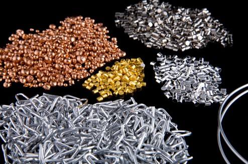
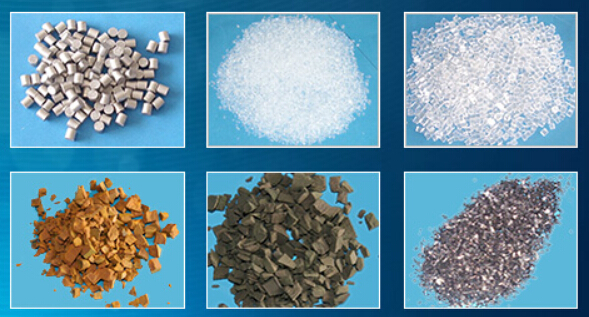
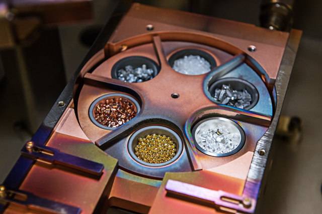
For more information about evaporation pellets, please follow our website or visit https://www.sputtertargets.net/evaporation-materials.html .

Thermal Evaporation History Part Three (From Mid 1900s to Late 1900s)

E-beam Evaporation Development

In 1949, Pierce described the “long-focus” electron beam gun for melting and evaporation in vacuum. The long focus gun suffers from shorting due to the deposition of evaporated material on the filament insulators that are in line-of-sight of the evaporating material. Deposition rates as high as 50 µm/s have been reported using e-beam evaporation. To avoid exposure of the filament to the vapor flux, bent-beam electron evaporators were developed.

In 1951, L. Holland patented the use of accelerated electrons to melt and evaporate the tip of a wire (“pendant drop”), which involved no filament or crucible.

In 1968, Hanks filed a patent on a 270° bent beam electron beam evaporation source that has become the most widely used design. Rastering the electron beam allows the energy of the electron beam to be distributed over the surface.

In 1970, Kurz was using an electron-beam system to evaporate gold for web coating. In electron beam evaporation a high negative “self-bias” can be generated on the surface of an insulating material or on an electrically isolated fixture. This bias can result in high-energy ion bombardment of the self-biased surface. 

In 1971, Chambers and Carmichael avoided that problem by having the beam pass through a small hole in a thin sheet in a section of a plate that separated the deposition chamber from the chamber where the filament was located. This allowed a plasma to be formed in the deposition chamber while the filament chamber was kept under a good vacuum. The plasma in the deposition chamber allowed ion bombardment of the depositing film material as well as “activation” of reactive gas.

In 1972, the uses of a hollow cathode electron emitter for e-beam evaporation was reported by J.R. Morley and H. Smith.

In 1978 H.R. Smith described a unique horizontally emitting electron beam (EB) vapor source. The source used a rotating crucible to retain the molten material, and its function was to coat large vertical glass plates. A number of thermoelectron-emitter e-beam source designs followed, including rod-fed sources and “multi-pocket” sources. The high voltage on the filament prevented the source from being used in a plasma where ions accelerated to the cathodic filament; this caused rapid sputter-erosion of the filament.

Crucible material Development

In 1951 Picard and Joy described the use of evaporation of materials from an RF-heated crucible. In 1966 Ames, Kaplan, and Roland reported the development of an electrically conductive TiB/BN composite ceramic (Union Carbide Co., UCAR™) crucible material that was compatible with molten aluminum.

Directed Deposition Development

The directed deposition is confining the vapor flux to one axis by eliminating off-axis components of the flux. Directed deposition can be attained by collimation of the vaporized material. In evaporation this was done by Hibi (1952), who positioned a tube between the source and the substrate. Collimation was also attained by H. Fuchs and H. Gleiter in their studies of the effects of atom velocity on film formation using a rotating, spiral-groove, velocity selector. In 1983, Ney described a source that emitted a gold atom beam with a 2° divergence. Recently “directed deposition” has been obtained using a flux of thermal evaporated material projected into a directed gas flow.

Thermally Evaporating Development

When thermally evaporating alloys, the material is vaporized with a composition in accordance with Raoult’s Law (1887). This means that the deposited film will have a continuously varying composition unless very strict conditions are met as to the volume of the molten pool using a replenishing source. One way of avoiding the problem is by “flash evaporation” of small volumes of material.

In 1948, L. Harris and B.M. Siegel reported flash evaporation by dropping small amounts of material on a very hot surface so that all of the material was vaporized before the next material arrived on the hot surface.

In 1964, Smith and Hunt described a method for depositing continuous strips of alloy foils by evaporation. Other free-standing thin-film structures are also deposited, such as beryllium Xray windows and nuclear targets.

To learn more about the history of thermal evaporation, please follow our website. We will update articles about evaporation pellets every week, so stay tuned. If you want to buy high quality evaporating pellets, please visit our official website for coating materials at https://www.sputtertargets.net/evaporation-materials.html.

Thermal Evaporation History Part Two (From early 1900s to mid 1900s)

In 1912 von Pohl and Pringsheim reported forming films by evaporation materials in a vacuum from a magnesia crucible that was heated by a resistively heated foil surrounding the crucible. They are sometimes credited with the first deposition by thermal evaporation in vacuum. In 1913, Langmuir studied the vaporization rate of materials in vacuum and also reported forming films.

Ritschl is often credited with being the first to use evaporation from a filament to form a film in vacuum. He reported thermal evaporation of silver from a tungsten wire basket to form half-silvered mirrors in 1931. Cartwright and Strong reported evaporating metals from a tungsten wire basket in the same year, but the technique they tried was not successful for evaporating aluminum because molten aluminum wets and alloys with the tungsten wire, which causes it to “burn out” when there is a relatively large volume of molten aluminum.  

Aluminum was not successfully evaporated until 1933 when John Strong used heavy-gauge tungsten wire that was wetted by the molten aluminum. John did a great deal of development using thermal evaporation of aluminum from multiple tungsten filaments for coating astronomical mirrors. Strong, with the help of designer Bruce Rule, aluminum coated the 200” Palomar astronomical telescope mirror in 1947 using multiple filaments and a 19-foot diameter vacuum chamber.

In 1817, Fraunhoffer noted that optical lenses improved with age due to the formation of a surface film. Following this discovery many investigators artificially aged lenses to form antireflection coatings. For example, in 1904 H.D. Taylor patented (British) an acid treatment of a glass surface in order to lower the index of refraction and the reflectivity by producing a porous surface. In 1933 A.H. Pfund vacuum-deposited the first single-layer (AR) coating (ZnS) while reporting on making beamsplitters and Bauer mentioned AR coatings in his work on the properties of alkali halides.

The Germans deposited CaF2 a nd MgF2 AR coatings during WWII. Plasma cleaning of glass surfaces is reported to have been used by Bauer at the Zeiss Company in 1934. The Schott Company (Germany) was also reported to have deposited three-layer AR coatings by flame-pyrolysis CVD during WWII.

In 1935, based on Bauer’s observation, A. Smakula of the Zeiss Company developed and patented AR coatings on camera lenses. The patent was immediately classified as a military secret and not revealed until 1940. In 1936 Strong reported depositing AR coatings on glass. In 1939 Cartwright and Turner deposited the first two-layer AR coatings. One of the first major uses of coated lenses was on the projection lenses for the movie Gone With the Wind, which opened in December 1939. The AR coated lenses gained importance in WWII for their light-gathering ability in such instruments as rangefinders and the Norden Bombsight.

The AR coated lenses gained importance in WWII for their light-gathering ability in such instruments as rangefinders and the Norden Bombsight. During WWII, baking of MgF2 films to increase their durability was developed by D.A. Lyon of the U.S. Naval Gun Factory. The baking step required that the lens makers coat the lens elements prior to assembly into compound lenses.

In 1943, the U.S. Army sponsored a conference on “Application of Metallic Fluoride Reflection Reducing Films to Optical Elements.” The proceedings of this conference are probably the first extensive publication on coating optical elements.

In 1958 the U.S. military formally approved the use of “vacuum cadmium plating” (VacCad) for application as corrosion protecmium. In recent years PVD processing has been used to replace electroplating in a number of applications to avoid the water pollution associated with electroplating.

To learn more about the history of thermal evaporation, please follow our website. We will update articles about evaporation pellets every week, so stay tuned. If you are interested in high quality evaporation pellets, please visit our official website for coating materials at https://www.sputtertargets.net/.

Thermal Evaporation History Part One (From late 1800s to early 1900s)

Thermal evaporation or vacuum evaporation is the vaporization of the evaporation material by heating to a certain temperature, so that the vapor pressure becomes appreciable, and the surface or molecules are lost from the surface in the vacuum. Vaporization can come from the surface of a liquid or from the surface of a solid. The authors arbitrarily define 10-2 Torr as the equilibrium vapor pressure above which the free surface evaporation in the PVD-type vacuum is sufficient to cause vacuum deposition to occur at a reasonable rate. If the evaporating material is a solid at this temperature, the material is said to be sublimed (e.g., chromium, magnesium), and if it is melted, it is said to evaporate (e.g., aluminum, molybdenum, tungsten). Some evaporation materials have a vapor pressure so that they can sublime or evaporate (e.g., titanium) at temperatures near their melting points. Some composites sublime and some evaporate.

Thermal Evaporation Materials. (Gold, Silver, Titanium, Silicon Dioxide, Tungsten, Copper)

Thermal evaporation studies in vacuum began in the late 19th century, beginning with the work of H. Hertz and S. Stefan, who determined the equilibrium vapor pressure – but they did not use the vapor am to form films.

In 1894, Thomas Edison‘s patent (applied in 1884) covered the vacuum evaporation of “heating to incandescence” and film deposition. He did not mention the evaporation of the molten material in his patent, and many materials did not evaporate at a perceptible rate before they were at or above their melting point. Edison did not use the process in any application, presumably because radiant heating from the source was detrimental to the vacuum materials available at the time.

In 1887, Nahrwold reported the formation of a platinum film by sublimation in a vacuum, which he was sometimes thought to use for the first time to form a film in vacuum using thermal evaporation.

In 1907, Soddy proposed to evaporate calcium onto the surface as a means of reducing the residual pressure in the sealed tube. This would be the first “reactive deposition” process.

In 1909, Knudsen proposed the “Knudsen Cosine Distribution Law” for vapor from a point source. In 1915, he refined the free surface evaporation rate as a function of equilibrium vapor pressure and ambient pressure. The resulting equation is called the Hertz-Knudsen surface equation for free-surface vaporization. Honig summarized the equilibrium vapor pressure data for 1957.

In 1917, Sturman reported using a silver-silver wire to deposit silver from a vacuum surface to form a mirror.

To learn more about the history of thermal evaporation, please follow our website. We will update articles about evaporation pellets every week, so stay tuned. If you want to buy high quality evaporating materials, please visit our official website for coating materials at https://www.sputtertargets.net/evaporation-materials.html.

Different Sizes and Shapes of Evaporation Materials

In physical vapor deposition coatings, sputtering targets and evaporation materials are two important types of raw materials. We can distinguish between the two materials by name and shape. First, the sputtering target is used for vacuum sputtering, and the evaporation material is used for vacuum evaporation. Secondly, the evaporating material is also called evaporation pellets because it is almost in the state of pellets or tablets during use, the shape of which can accelerate the evaporation rate and coating quality. The following picture can easily help you identify the target and evaporate.

sputtering target & evaporation materials

Although the evaporating materials are usually granular, there are also differences in their sizes and shapes.

Regular Shapes

Cylindrical evaporation pellets

The cylinder is the most common shape in the evaporating material particles. According to the length of the cylinder, it can be subdivided into the following three shapes:

Quadratic Cylinder. Its main axis has the same length as its equatorial axis. Its meridian plane is a square.

Elongated Cylinder. Its main axis is longer than its equatorial axis. Its meridian plane is a rectangle.

Shortened Cylinder. Its main axis is shorter than its equatorial axis. Its meridian plane is a rectangle.

different shapes of cylindrical evaporation pellets

Globular evaporation pellets

Square evaporation pellets

Irregular shapes

In fact, many of the evaporating materials for industrial applications are actually irregularly shaped evaporating materials. It cannot be said that which one (the regular or irregular) is better. The shape of the evaporating particles should be selected according to specific application and the specific materials. The following are the common irregular evaporation pellets.

Evaporation powder materials

Triangular evaporation pellets

Lamellar evaporation pellets

For more information, please visit https://www.sputtertargets.net/.

Evaporation Materials for Thin Film Coatings

Vacuum Evaporation is a form of physical vapor deposition (PVD) where material is heated to a high vapor pressure, often in molten state. Then, the vapors are condensed on to a substrate to form a desired thickness of a thin film. The heating is typically accomplished via resistive heating or by E-beam (electron beam). Materials used in the evaporation process to be heated are called evaporation materials, or evaporation pellets.

Evaporation Materials is Specifical for Evaporation

Evaporating materials are specially designed pellets for vacuum evaporation. They have a specific form factor and are intended to evaporate at a known rate. Typically during the evaporation process, “splashing” causes the droplet material to splash onto the substrate. Engineered granules are manufactured using specific metal purity and processes to minimize the incorporation of gases and impurities, thereby reducing “splashing” in the process.

Evaporation Materials Types & Application

The evaporation materials include (on raw materials): Metal Evaporation Material , Oxide Evaporation Material , Fluorid Evaporation Material, Boride evaporation materials, Carbide evaporation mateirals, nitrides evaporation materials, selenides evaporation materials, sulfides evaporation materials, tellurides evaporation materials, Other Compound Evaporation Material, Mixture Evaporation Material , alloy evaporation material. 

As one kinds of primary PVD coating material, Evaporation material are widely used for fields of optical, electric, photoelectric, decorate and so on. Users usually make cold light mirror, high reflective coating, anti-reflective coating and laser coating etc.

Vacuum Evaporation Coating Website works for Stanford Advanced Materials. You can visit https://www.sputtertargets.net/ for high quality evaporation materials.

Design a site like this with WordPress.com
Get started